Serial transmitter.
modified:10 September 2024 04:21:09.
Purpose:
This is Verilog code is a Serial transmitter, it purpose is to transmit 8-bit bytes over a serial link.
The 'ready' signal indicates that the 'cached' byte, has been moved to the shift register, and is now empty and can be loaded with another byte.
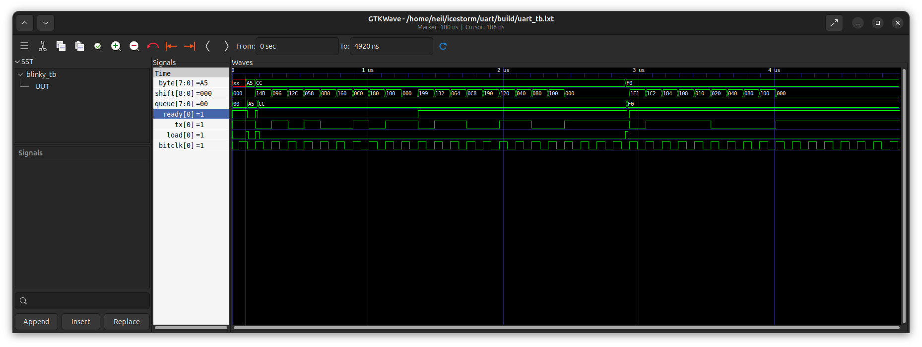
Waveform capture of the Testbench:
This is a waveform capture of the testbench.
First a 0xA5 is loaded into the cache, this is almost imediately transfered into the shift register.
Next a 0xCC is loaded into the cache, but as the first byte is still being transmitted, it stays in the cache for a while, approx. 1.4uS.
Lastly at about the 2.9uS the last byte is transfered into the cache.
 Waveform
The Testbench:
The Testbench isn't very sophisticated. It main purpose is to control the 'load' signal.
`timescale 1ns/1ns
module serial_tb;

  reg tClk = 1'b0;
  wire tLed1;
  reg [7:0] byte;
  reg load = 0;
  wire ready;

  top #(.DIVIDER(2)) UUT
  (
    .clk_in(tClk),
    .byte(byte),
    .load(load),
    .ready(ready),
    .tx(tLed1)
  );

  always #10 tClk <= !tClk;  // 48MHz

  initial
	begin
		$dumpfile("build/uart_tb.lxt");
		$dumpvars(0,serial_tb);
	end

	initial
	begin
		#100;
		wait (ready == 1);
		byte = 8'hA5;
		load = 1;
		wait (ready == 0);
		#10
		load = 0;

		wait (ready == 1);
		byte = 8'hCC;
		load = 1;
		wait (ready == 0);
		#10
		load = 0;

		#2700;

		wait (ready == 1);
		byte = 8'hF0;
		load = 1;
		wait (ready == 0);
		#10
		load = 0;

		#2000;
		$finish;
	end
endmodule
Serial Trasmitter module:
The internal clock of the FPGA is 48MHz.
The formula for the buad rate counter is therefor:
MHz / buadrate / 2 = divider
48000000 / 115200 / 2 = 208
load = the incomming signal to load the cache register.
ready = an outgoing signal to indicate that the cache is empty.
tx = the output serial bit.
This uses a 9-bit shift register, 8-bits of data + 1 stop bit. This makes it easier to know when to stop transmitting the bits.
The state machine has only 2 states, so a 1-bit register is used for the FSM.
module top #(parameter integer DIVIDER = 208) (input clk_in,		// defualt 48MHz
			input [7:0] byte,
			input load,
			output ready,
			output tx);
	reg [7:0] counter = 0;				// 8-bit counter
	reg bitclk = 0;
	reg [7:0] queue = 0;
	reg queue_full = 0;
	reg [8:0] shift = 0;				// data + stop bit
	reg bit = 1;						// idle condition

	assign tx = bit;
	assign ready = !queue_full;

	localparam WAITING = 0,
			RUNNING = 1;
	reg  state = WAITING;

	always @ (posedge clk_in) begin
		// gerate the bitclock
		if (counter == DIVIDER) begin		// changes state ever 4350nS
			counter <= 0;
			bitclk <= !bitclk;			// this is so the clock has 50% duty
		end
		else begin
			counter <= counter + 1;
		end
		if (load && !queue_full) begin
			queue <= byte;
			queue_full <= 1;
		end
	end

	always @ (posedge bitclk) begin
		case (state)
			WAITING: begin
				if (queue_full) begin
					shift[8:1] <= queue;
					shift[0] <= 1;
					bit <= 0;					// output start bit
					state <= RUNNING;
					queue_full <= 0;			// reset the queue full flag
				end
			end
			RUNNING: begin
				bit <= shift[8];
				shift[8:1] <= shift[7:0];
				shift[0] <= 0;
				if (shift == 0) begin
					if (queue_full) begin
						shift[8:1] <= queue;	// data
						shift[0] <= 1;			// stop bit
						bit <= 0;				// output start bit
						queue_full <= 0;		// reset the queue full flag
					end
					else begin
						state <= WAITING;
						bit <= 1;
					end
				end
			end
		endcase
	end
endmodule